社区
驱动开发/核心开发
帖子详情
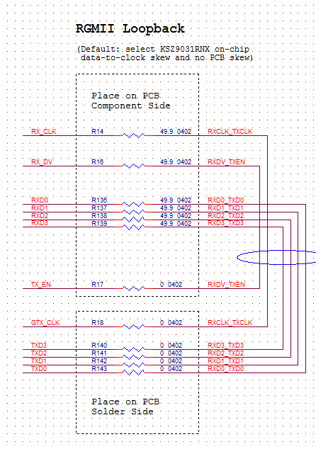
关于RMII和MII接口Loopback的问题
wanyug
2017-09-28 06:52:51
请问 RMII 或者 MII接口的 TXD、TX_EN 与RXD、RS_DV可否进行对接(环回测试),能否正常通信?
谢谢
...全文
996
3
打赏
收藏
关于RMII和MII接口Loopback的问题
请问 RMII 或者 MII接口的 TXD、TX_EN 与RXD、RS_DV可否进行对接(环回测试),能否正常通信? 谢谢
复制链接
扫一扫
分享
转发到动态
举报
写回复
配置赞助广告
用AI写文章
3 条
回复
切换为时间正序
请发表友善的回复…
发表回复
打赏红包
zhxianbin
2017-10-09
打赏
举报
回复
作loopback测试,mac,phy都可以设置的,不需要硬件定死
weixin_40500893
2017-10-07
打赏
举报
回复
可以,但是一般芯片内部可以通过设置寄存器连接测试 --Linux星球
e-love
2017-09-30
打赏
举报
回复
可以的、、
uart_
loopback
_上位机zynq_FPGAverilog_verilogUart_zynquart_
实现zynq与电脑上位机串口终端的数据换回
RTL8309M-CG_Datasheet
The RTL8309M-CG is a 9-port 10/100M Ethernet switch controller that integrates memory, nine MACs, and eight physical layer transceivers for 10Base-T and 100Base-TX operation into a single chip. It supports a (T)
MII
/R
MII
interface for external devices to connect to the 9th MAC. The external device could be a routing engine, HomePNA, HomePlug, or VDSL transceiver depending on the application. In order to accomplish diagnostics in complex network systems, the RTL8309M provides a
loopback
feature in each port.
RTL8306E-CG_Realtek.pdf
RTL8306E-CG规格书。The RTL8306E-CG is a 6-port Fast Ethernet switch controller that integrates memory, six MACs, and five physical layer transceivers for 10Base-T and 100Base-TX operation into a single chip. The RTL8306E supports a Dual
MII
/R
MII
interface for external devices to connect to the 6th MAC, 5th MAC, and 5th PHY. The external device could be a routing engine, HomePNA, HomePlug, or VDSL transceiver depending on the application. In order to accomplish diagnostics in complex network systems, the RTL8306E provides a
loopback
feature in each port. The RTL8306E supports several advanced QoS functions with four-level priority queues to improve multimedia or real-time networking applications, including: • Multi-priority assignment • Differential queue weight • Port-based and queue-based rate limitation • 16-entry ACL for advanced packet control application
DP83848CVV.pdf
National_Semiconductor的一款网络芯片的技术手册。1.0 Pin Descriptions m 9 1.1 Serial Management Interface 9 1.2 MAC Data Interface .9 1.3 Clock Interface 11 1. 4 LED Interface 1.5 Reset and Power down 12 1.6 Strap Options 12 1.7 10 Mb/s and 100 Mb/s PMD Interface 14 1.8 Special Connections 14 1. 9 Power Supply Pi 14 1. 10 Package Pin AsSi 15 2.0 Configuration 16 2. 1 Auto-Negotiation g 16 2.1.1 Auto-Negotiation Pin Control 16 2.1.2 Auto-Negotiation Register Control 16 2.1.3 Auto-Negotiation Parallel Detection 2. 1. 4 Auto-Negotiation Restart 2.1.5 Enabling Auto-Negotiation via Software 17 2.1.6 Auto-Negotiation Complete Time 17 2.2 Auto-MDIX 2. 3 PHY Address 18 2.3.1 Mll Isolate mode 2.4 LED Interface 19 2.4.1LED 19 2.4.2 LED Direct Control 2.5 Half Duplex VS Full Duplex 20 2.6 Internal
Loopback
20 2.7 BIST 20 3.0 Functional Description .I.I... 21 3.1 Mll Interface 3.1.1 Nibble-wide mll data Interface 21 3.1.2 Collision detect 3.1.3 Carrier Sense 21 3.2 Reduced mll Interface 3.3 10 Mb Serial Network Interface(SNI) .22 3. 4 802.3u Mll Serial Management Interface 3.4.1 Serial Management Register Access 3.4.2 Serial Management Access protocol 22 3.4.3 Serial Management Preamble Suppression 4.0 Architecture 24 4.1100BASE-TX TRANSMITTER .24 4.1. 1 Code-group Encoding and Injection 26 4.1.2 Scrambler 26 4.1 3 Nrz to nrzi Encoder 26 4.1. 4 Binary to MLT-3 Convertor 26 4.2100 BASE-T×RECEⅣVER 26 4.2.1 Analog Front Et 26 4.2.2 Digital Signal Processor 26 4.2.2.1 Digital Adaptive Equalization and gain Control 28 4.2.2.2 Base Line Wander Compensation 4.2.3 Signal detect 4.2.4 MLT-3 to nrzi Decoder 4,25 nrz to nrz 4.2.6 Serial to parallel 4.2.7 Descrambler 4.2.8 Code-group Alignment 4.29 4B/5B Decoder 4.2. 10 100BASE-TX Link Integrity Monitor ..30 42. 11 Bad ssD Detection .30 www.national.com Oo寸∞∞∞ 4.3 10BASE-T TRANSCEIVER MODULE 30 4.3.1 Operational Modes 30 4.3.2 Smart squelch 31 4.3.3 Collision Detection and sQE 4.3.4 Carrier Sense 31 4.3.5 Normal Link Pulse detection/Generation 4.3.6 Jabber function …32 4.3. 7 Automatic Link Polarity detection and correction .....32 4.3.8 Transmit and Receive Filtering ...32 4.3.9 Transmitter 4.3.10 Receiver 5.0 Design Guidelines 33 5. 1 TPI Network circuit ....33 5.2 ESD Protection 34 5.3 Clock In(X1) Requirements 34 5. 4 Power feedback circu 35 5.5 Power Down/Interrupt 35 5.5.1 Power down control mode ....35 5.5.2 Interrupt Mechanisms 5.6 Energy Detect Mode 36 6.0 Reset Operation..∴.∴∴∴.37 6.1 Hardware reset 6.2 Software reset 7.0 Register Block ,,,,,,,,,38 7. 1 Register definition 7.1.1 Basic Mode Control Register(BMCR) 7.1.2 Basic Mode Status Register(BMSR) 44 7.1.3 PHY Identifier Register #1 (PHYIDR1) 45 7.1. 4 PHY Identifier Register #2(PHYIDR2 ..45 7.1.5 Auto-Negotiation Advertisement Register(ANAR) .......45 7.1.6 Auto-Negotiation Link Partner Ability Register(ANLPAR) (BASE Page) 7.1.7 Auto-Negotiation Link Partner Ability Register(ANLPAR)(Next Page) 7.1.8 Auto-Negotiate Expansion Register (ANER) 7.1.9 Auto-Negotiation Next Page Transmit Register(ANNPTR) 7.2 EXtended Registers 50 7.2.1 PHY Status Register(PHYSTS 7.2.2 Mll Interrupt Control Register(MICR 52 7.2.3 MIl Interrupt Status and Misc. Control Register(MISR) 7.2.4 False Carrier Sense Counter Register(FCSCR) 7.2.5 Receiver Error Counter Register(RECR 7.2.6 100 Mb/s PCS Configuration and Status Register(PCSR) 55 7.2.7 R
MII
and Bypass Register(RBR) 7. 2. 8 LED Direct Control Register(LEDCR 7. 2. 9 PHY Control Register(PHYCR) .....57 7.2.10 10Base-T Status/Control Register(1OBTSCR) 58 7. 2.11 CD Test and BIST Extensions Register(CDCTRL1) 60 7. 2. 12 Energy Detect Control (EDCR) 6 8.0 Electrical Specifications 62 8.1 DC Specs 62 8.2 AC Specs .,,,,.,64 8.2.1 Power Up Timing 64 8.2.2 Reset Timing 8.2.3 Mll Serial Management Timing 8.2.4 100 Mb/s MIl Transmit Timing 8.2.5 100 Mb/s Mll Receive Timing ............67 8.2.6 100BASE-TX Transmit Packet Latency Timing 67 8.2.7 100BASE-TX Transmit Packet Deassertion Timing 8.2.8 100BASE-TX Transmit Timing(tr/F& Jitter) 8.2.9 100BASE-TX Receive Packet Latency Timing 70 8.2.10 100BASE-TX Receive Packet Deassertion Timing 70 www.national.com 8.2.11 10 Mb/s Mll Transmit Timing 71 8.2.12 10 Mb/s Mll Receive Timing 8.2.13 10 Mb/s serial Mode Transmit Timing 8.2.14 10 Mb/s serial Mode Receive timing 8.2.15 10BASE-T Transmit Timing (Start of Packet 73 8.2. 16 10BASE-T Transmit Timing(End of Packet 73 8. 2. 17 10BASE-T Receive Timing(Start of Packet) 8.2.18 10BASE-T Receive Timing(End of Packet 74 8.2.19 10 Mb/s heartbeat Timing 75 8.2.20 10 Mb/s Jabber Timing 8222 Auto-Negotiation Fast Link Pulse(FLP) Timing…、∴ 8.2.21 10BASE-T Normal Link Pulse Timing .....,,,,76 8.2.23 100BASE-TX Signal Detect Timing 8.2.24 100 Mb/s Internal
loopback
timing 8.2.25 10 Mb/s Internal
Loopback
Timing .78 8. 2.26 R
MII
Transmit Timing .79 8.2.27 R
MII
Receive Timing 82.28 Isolation Timing 81 8.2.29 25 MHz OUT Timing 81 8.2.30 100 Mb/s X1 to TX CLK Timing 82 9.0 Physical Dimensions∴∴ ■■■ 84 ww.national. com Oo寸∞∞∞ List of Figures Figure 1. DP83848C Functional Block Diagram..... Figure 2. PHYAD Strapping Example 18 Figure 3. AN Strapping and LED Loading Example 19 Figure 4. Typical MDC/MDIO Read Operation ......23 Figure 5. Typical MDC/MDIO Write Operation 23 Figure 6. 100BASE-TX Transmit Block Diagram ,,,,,,.,,.24 Figure 7. 100BASE-TX Receive Block Diagram 27 Figure 8. EIA/TIA Attenuation Vs Frequency for 0, 50, 100, 130&150 meters of CAt 5 cable...... 28 Figure 9. 100BASE-TX BLW Event ........ Figure 10. 10BASE-T Twisted Pair Smart Squelch Operation 31 Figure 11 10/100 Mb/s Twisted Pair Interface...,.......... 33 Figure 12. Crystal Oscillator Circuit 34 Figure 13. Power Feeback Connection 35 www.national.com List of tables Table 1. Auto-Negotiation Modes .16 Table 2. PHY Address Mapping Table 3. lEd Mode select 19 Table 4. Supported packet sizes at +/-50ppm +/-100ppm for each clock Table 5. Typical MDIO Frame Format Table 5. 4B5B Code-Group Encoding/Decoding Table 6. 25 .,34 Table7.25 MHz Oscillator Specification∴.∴.∴ ,,,,,,,,,,34 Table 8. 50 MHz Oscillator Specification ,,35 Table 9. 25 MHz Crystal Specification Table 10 Register Map...................... 38 Table 11. Register Table ..∴......39 Table 12. Basic Mode Control Register (BMCR), address 0X00 Table 13. Basic Mode Status Register(BMSR), address 0x01 Tabe14. PHY ldentifier Register#1( PHYIDR1), address0x02.∴………………………4 Table 15 PHY Identifier Register #2 (PHYIDR2), address 0x03 45 Table 16. Negotiation Advertisement Register(ANAR), address 0x04 45 Table 17. Auto-Negotiation Link Partner Ability Register(ANLPAR)(BASE Page), address 0x05.... 46 Table 18 Auto-Negotiation Link Partner Ability Register(ANLPAR)(Next Page), address 0x05..... 48 Table 19. Auto-Negotiate Expansion Register(ANER), address 0X06 Table 20 Auto-Negotiation Next Page Transmit Register(ANNPTR), address 0x07 .∴.∴......,49 Table 21. PHY Status Register(PHYSTS), address 0x10 Table 22 Mll Interrupt Control Register(MICR), address 0x11 n..52 Table 23. MIl Interrupt Status and Misc. Control Register(MISR), address 0x12 .....∴.53 Table 24. False Carrier Sense Counter Register(FCSCR), address 0x14 54 Table 25 Receiver Error Counter Register(RECR), address 0x15 54 Table 26. 100 Mb/s PCS Configuration and Status Register(PCSR), address 0x16 Table 27.
RMI
and Bypass Register(RBR), addresses 0x17...................56 Table 28 LED Direct Control Register (LEDCR), address 0X18 量重面 重重m 56 Table 29 PHY Control Register(PHYCR), address Ox19 57 Table 30 10Base-T Status/Control Register(10BTSCR), address OX1A Table 31. CD Test and BIST Extensions Register(CDCTRL1), address 0x1B ..60 Table 32. Energy Detect Control (EDCR), address 0x1D ,,61 www.national.com Oo寸∞∞∞ In Layou 乙uzoOHOau PFBIN2 24 RBIAS 23上 PFBOU RX DV/MIL MODE AVDD33 CRS/CRS DV/LED CFG RESERVED RX ER/MDIX EN 41 RESERVED 42 RXD O/PHYAD1 DP838480 PFBIN1 RXD 1/PHYAD2 Td RXD 2/PHYAD3 TD RXD 3/PHYAD4 AGND OGND JOVDD33 Hz=z3oa au>u c u>uOu p vie NS Package Number Vbh48A www.national.com 1.0 Pin Descriptions The DP83848C pins are classified into the following inter- All DP83848C signal pins are i/o cells regardless of the face categories(each interface is described in the sections particular use. The definitions below define the functionality that follow of the l/O cells for each pin Serial Management Interface Input MAC Data Interface Output Clock Interface Type: I/o Input/Output LED Interface Type OD Open Drain Reset and power down Type: PD, PU Internal Pulldown/Pullup Strap Options Strapping Pin(All strap pins have weak in- --10/100 Mb/s Pmd Interface ternal pull-ups or pull-downs. If the default Special Connect Pins strap value is needed to be changed then an external 2.2 k resistor should be used Power and ground pins Please see Section 1.6 for details.) Note: Strapping pin option. Please see Section 1.6 for strap definitions 1.1 Serial Management Interface Signal Name Tvpe Pin t Description MDC 31 MANAGEMENT DATA CLOCK: Synchronous clock to the MDIo management data input/output serial interface which may be asynchronous to transmit and receive clocks. The maximum clock rate is 25 Mhz with no minimum clock rate MDIO 30 MANAGEMENT DATA l/O: Bi-directional management instruc tion/data signal that may be sourced by the station management entity or the PhY. This pin requires a 1.5k pullup resistor 1.2 MAC Data Interface Signal name Type Pin t Description TX CLK
MII
TRANSMIT CLOCK: 25 MHz Transmit clock output in 100 Mb/s mode or 2.5 MHz in 10 mb/s mode derived from the 25 mHz reference clock Unused in emil mode the device uses the x1 reference clock in put as the 50 MHz reference for both transmit and receive SNI TRANSMIT CLOCK: 10 MHZ Transmit clock output in 10 Mb SNI mode. The MAc should source TX EN and TXdO using this clock TX EN L PD Mll TRANSMIT ENABLE: Active high input indicates the pres ence of valid data inputs on TXD3: 0 R
MII
TRANSMIT ENABLE: Active high input indicates the pres- ence of valid data on TXD[1: 0 SNI TRANSMIT ENABLE: Active high input indicates the pres- ence of valid data on TXD 0 TXD 0
MII
TRANSMIT DATA: Transmit data Mll input pins, TXD3: 0 TXD 1 3456 that accept data synchronous to the TX ClK (2.5 MHz in 10 Mb/s mode or 25 MHz in 100 Mb/s mode) TXD 2 R
MII
TRANSMIT DATA: Transmit data R
MII
input pins, TXD[1 TXD 3 S.L. PD that accept data synchronous to the 50 MHz reference clock SNI TRANSMIT DATA: Transmit data sNi input pin TXd 0, that accept data synchronous to the TX CLK (10 MHz in 10 Mb/s sni mode) www.national.com Oo寸∞∞∞ Signal name Type Pin #i Description RX CLK 38 MI RECEE CLOCK: Provides the 25 mhz recovered receive clocks for 100 Mb/s mode and 2.5 MHz for 10 Mb/s mode Unused in rmll mode the device uses the xl reference clock in put as the 50 MHz reference for both transmit and receive SNI RECEIVE CLOCK: Provides the 10 MHz recovered receive clocks for 10 Mb/s sni mode RXD∨ S.O. PD
MII
RECEIVE DATA VALID: Asserted high to indicate that valid data is present on the corresponding RXD[3: 0]. MIl mode by de fault with internal pulldown R
MII
Synchronous Receive Data Valid: This signal provides the R
MII
Receive Data valid indication independent of carrier sense This pin is not used in SNI mode RX ER S.O. PU MIl RECEIVE ERROR: Asserted high synchronously to RX CLK to indicate that an invalid symbol has been detected within a re ceived packet in 100 Mb/s mode R
MII
RECEIVE ERROR: Assert high synchronously to X1 when- ever it detects a media error and rxdv is asserted in 100 mb/s This pin is not required to be used by a mac, in either mil or rmll mode, since the Phy is required to corrupt data on a receive error This pin is not used in SNI mode RXD O S.O. PD
MII
RECEIVE DATA: Nibble wide receive data signals driven syn RXd 1 chronously to the rx clk, 25 Mhz for 100 Mb/s mode 2.5 MHZ for 10 Mb/s mode ) RXD[3 0] signals contain valid data when RXD 2 45 RX DV is asserted RXD 3 46 R
MII
RECEIVE DATA: 2-bits receive data signals, RXD[1: 0], driv en synchronously to the X1 clock, 50 MHZ SNI RECEIVE DATA: Receive data signal, RXD 0, driven syn chronously to the RX ClK RXd0 contains valid data when CRs is asserted. RXD[3: 1] are not used in this mode CRS/CRS DV S.O. PU
MII
CARRIER SENSE: Asserted high to indicate the receive me dium is non idle R
MII
CARRIER SENSE/RECEIVE DATA VALID: This signal combines the rmll carrier and receive data valid indications For a detailed description of this signal, see the R
MII
Specifica- SNI CARRIER SENSE: Asserted high to indicate the receive me dium is non -idle. It is used to frame valid receive data on the RXD 0 signal COL S.O. PU MI COLLISION DETECT: Asserted high to indicate detection of a collision condition(simultaneous transmit and receive activity) in 10 Mb/s and 100 Mb/s Half Duplex Modes While in 10BASE-T Half Duplex mode with heartbeat enabled this pin is also asserted for a duration of approximately 1 s at the end of transmission to indicate heartbeat (SQE test In Full duplex Mode, for 10 Mb/s or 100 Mb/s operation, this sig nal is always logic 0. There is no heartbeat function during 10 Mb/s full duplex operation R
MII
COLLISION DETECT: Per the RMll Specification, no COL signal is required. The MAc will recover CRS from the CRS DV signal and use that along with its tX en signal to dete
rmi
ne col- SNI COLLISION DETECT: Asserted high to indicate detection of a collision condition(simultaneous transmit and receive activity) in 10 Mb/s sni mode www.national.com 10
以太网RG
MII
/
MII
/R
MII
接口
回环测试方案
1、模组的MAC通过RG
MII
/
MII
/R
MII
接口
与PHY连接2、MAC层数据经过RG
MII
到达PHY的PCS层3、设置PHY的PCS层回环,使PCS层数据回到MAC层4、判断MAC层TX与RX接收的数据。如果MAC能接收到数据,测试PASS,否则失败。
驱动开发/核心开发
21,597
社区成员
21,709
社区内容
发帖
与我相关
我的任务
驱动开发/核心开发
硬件/嵌入开发 驱动开发/核心开发
复制链接
扫一扫
分享
社区描述
硬件/嵌入开发 驱动开发/核心开发
社区管理员
加入社区
获取链接或二维码
近7日
近30日
至今
加载中
查看更多榜单
社区公告
暂无公告
试试用AI创作助手写篇文章吧
+ 用AI写文章


 发帖
发帖 与我相关
与我相关 我的任务
我的任务
 分享
分享