社区
Java EE
帖子详情
PO,VO,Relationship
闲去野鹤
2013-10-08 03:32:49
谁能看懂这图?请赐教
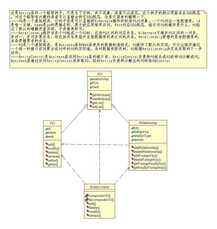
...全文
96
3
打赏
收藏
PO,VO,Relationship
谁能看懂这图?请赐教
复制链接
扫一扫
分享
转发到动态
举报
写回复
配置赞助广告
用AI写文章
3 条
回复
切换为时间正序
请发表友善的回复…
发表回复
打赏红包
闲去野鹤
2013-10-09
打赏
举报
回复
别沉呀, 我想问的是: 如果应用程序增加一个VO,Business层怎么调用EntityControl,EntityControl如何分解VO,怎么访问Relationship,怎么处理PO,怎么访问DBControl层?
闲去野鹤
2013-10-08
打赏
举报
回复
引用 1 楼 songbgi 的回复:
猛的一看 感觉就像 主表 明细表 vo是主 po是明细
能否给个示例?vo是业务上的一个虚拟的对象,po是与数库存表一一对应的真实实体。那维护他们之间关系的relationship是怎么维护的?
身胖不怕影子歪
2013-10-08
打赏
举报
回复
猛的一看 感觉就像 主表 明细表 vo是主 po是明细
0.96OLED显示屏数据手册
Pin Number Symbol I/O Function P
Po
o we er r S Su up pp pl ly y 9 VDD P P
Po
o we er r S Su up pp pl ly y f fo or r L Lo og gi ic c This is a
vo
ltage supply pin. It must be connected to external source. 8 VSS P G Gr ro ou un nd d o of f L Lo og gi ic c C Ci ir rc cu ui it t This is a ground pin. It acts as a reference for the logic pins. It must be connected to external ground. 28 VCC P P
Po
o we er r S Su up pp pl ly y f fo or r OE EL L P Pa an ne el l This is the most
po
sitive
vo
ltage supply pin of the chip. A stabilization capacitor should be connected between this pin and V SS when the converter is used. It must be connected to external source when the converter is not used. 29 VLSS P G Gr ro ou un nd d o of f A An na al lo og g C Ci ir rc cu ui it t This is an analog ground pin. It should be connected to V SS externally. D Dr ri iv ve er r 26 IREF I C Cu ur rr re en nt t R Re ef fe er re en nc ce e f fo or r B Br ri ig gh ht tn ne es ss s A Ad dj ju us st t me en nt t This pin is segment current reference pin. A resistor should be connected between this pin and V SS . Set the current at 12.5μA maximum. 27 VCOMH O V
Vo
ol lt ta ag ge e Ou ut tp pu ut t Hi ig gh h L Le ev ve el l f fo or r C C O M S Si ig gn na al l This pin is the input pin for the
vo
ltage output high level for COM signals. A capacitor should be connected between this pin and V SS . D DC C/ /D DC C C Co on nv ve er rt te er r 6 VDDB P P
Po
o we er r S Su up pp pl ly y f fo or r DC C/ / DC C C Co on nv ve er rt te er r C Ci ir rc cu ui it t This is the
po
wer supply pin for the internal buffer of the DC/DC
vo
ltage converter. It must be connected to external source when the converter is used. It should be connected to V DD when the converter is not used. 4 / 5 2 / 3 C1P / C1N C2P / C2N I P
Po
os si it ti iv ve e T Te er r mi in na al l o of f t th he e F Fl ly yi in ng g I In nv ve er rt ti in ng g C Ca ap pa ac ci it to or r Ne eg ga at ti iv ve e T Te er r mi in na al l o of f t th he e F Fl ly yi in ng g B Bo oo os st t C Ca ap pa ac ci it to or r The charge-pump capacitors are required between the terminals. They must be floated when the converter is not used. I In nt te er rf fa ac ce e 10 11 12 BS0 BS1 BS2 I C Co o m mu un ni ic ca at ti in ng g P Pr ro ot to oc co ol l S Se el le ec ct t These pins are MCU interface selection input. See the following table: BS0 BS1 BS2 I 2 C 0 1 0 3-wire SPI 1 0 0 4-wire SPI 0 0 0 8-bit 68XX Parallel 0 0 1 8-bit 80XX Parallel 0 1 1 14 RES# I P
Po
o we er r R Re es se et t f fo or r C Co on nt tr ro ol ll le er r a an nd d Dr ri iv ve er r This pin is reset signal input. When the pin is low, initialization of the chip is executed. Keep this pin pull high during normal operation. 13 CS# I C Ch hi ip p S Se el le ec ct t This pin is the chip select input. The chip is enabled for MCU communication only when CS# is pulled low. 15 D/C# I Da at ta a/ /C Co o m ma an nd d C Co on nt tr ro ol l This pin is Data/Command control pin. When the pin is pulled high, the input at D7~D0 is treated as display data. When the pin is pulled low, the input at D7~D0 will be transferred to the command register. When the pin is pulled high and serial interface mode is selected, the data at SDIN will be interpreted as data. When it is pulled low, the data at SDIN will be transferred to the command register. In I 2 C mode, this pin acts as SA0 for slave address selection. For detail
relationship
to MCU interface signals, please refer to the Timing Characteristics Diagrams. 17 E/RD# I R Re ea ad d/ / Wr ri it te e E En na ab bl le e o or r R Re ea ad d This pin is MCU interface input. When interfacing to a 68XX-series microprocessor, this pin will be used as the Enable (E) signal. Read/write operation is initiated when this pin is pulled high and the CS# is pulled low. When connecting to an 80XX-microprocessor, this pin receives the Read (RD#) signal. Data read operation is initiated when this pin is pulled low and CS# is pulled low. When serial or I 2 C mode is selected, this pin must be connected to V SS . GoldenMorning Electronic 4 1.5 Pin Definition (Continued) Pin Number Symbol I/O Function I In nt te er rf fa ac ce e ( (C Co on nt ti in nu ue ed d) ) 16 R/W# I R Re ea ad d/ / Wr ri it te e S Se el le ec ct t o or r Wr ri it te e This pin is MCU interface input. When interfacing to a 68XX-series microprocessor, this pin will be used as Read/Write (R/W#) selection input. Pull this pin to “High” for read mode and pull it to “Low” for write mode. When 80XX interface mode is selected, this pin will be the Write (WR#) input. Data write operation is initiated when this pin is pulled low and the CS# is pulled low. When serial or I 2 C mode is selected, this pin must be connected to V SS . 18~25 D0~D7 I/O Ho os st t Da at ta a I In np pu ut t/ / Ou ut tp pu ut t B Bu us s These pins are 8-bit bi-directional data bus to be connected to the microprocessor’s data bus. When serial mode is selected, D1 will be the serial data input SDIN and D0 will be the serial clock input SCLK. When I 2 C mode is selected, D2 & D1 should be tired together and serve as SDA out & SDA in in application and D0 is the serial clock input SCL. Unused pins must be connected to V SS except for D2 in serial mode. R Re es se er rv ve e 7 N.C. - R Re es se er rv ve ed d P Pi in n The N.C. pin between function pins are reserved for compatible and flexible design. 1, 30 N.C. (GND) - R Re es se er rv ve ed d P Pi in n ( (S Su up pp
po
or rt ti in ng g P Pi in n) ) The sup
po
rting pins can reduce the influences from stresses on the function pins. These pins must be connected to external ground as the ESD protection circuit.
Java中
VO
、
PO
、DO、DTO、 BO、 QO、DAO、
PO
JO的概念
Java中
VO
、
PO
、DO、DTO、 BO、 QO、DAO、
PO
JO的概念
框架 day38 SVN安装及使用,SSH练习项目CRM,环境搭建(myeclipse hibernate 反转引擎生成
PO
和映射)
框架 day38 SVN安装及使用,SSH练习项目CRM,环境搭建(myeclipse hibernate 反转引擎生成
PO
和映射)
DO、DTO、
VO
、
PO
JO使用场景
model,entity,dto,viewmodel这些新手比较迷茫到底有什么区别,说白了都是一个类,里面有些属性字段。 那怎么区分他们,我说的简单点吧,我的理解是这样的: model是一个模型,里面装了各种数据,将一个model传递给view,在试图页面就可以使用model里面的数据来呈现到页面上。 而entity是实体,就是和数据表一一对应的,一个实体一张表。 官方的demo没有entity这...
java 常用缩写简表_java中的
po
等缩写解释
java中常用英文简写全拼与中文意思_计算机软件及应用_IT/计算机_专业资料。...信号缩写解释_文学_高等教育_教育专区。ACC AM AP ARB ARC AR...Fab内部情况及缩写解释_信息与通信_工程科技_专业资料。半导体从业人员都可以看看!还附有半导体相关英文缩写解释! 的基本知识(想入此行当的朋友请先) [分享]半导体......英文缩写及解释_英语学习_外语学习_教育专区。Ab...
Java EE
67,513
社区成员
225,880
社区内容
发帖
与我相关
我的任务
Java EE
J2EE只是Java企业应用。我们需要一个跨J2SE/WEB/EJB的微容器,保护我们的业务核心组件(中间件),以延续它的生命力,而不是依赖J2SE/J2EE版本。
复制链接
扫一扫
分享
社区描述
J2EE只是Java企业应用。我们需要一个跨J2SE/WEB/EJB的微容器,保护我们的业务核心组件(中间件),以延续它的生命力,而不是依赖J2SE/J2EE版本。
社区管理员
加入社区
获取链接或二维码
近7日
近30日
至今
加载中
查看更多榜单
社区公告
暂无公告
试试用AI创作助手写篇文章吧
+ 用AI写文章


 发帖
发帖 与我相关
与我相关 我的任务
我的任务
 分享
分享
